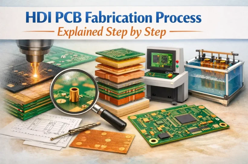

HDI PCB Fabrication Process Explained Step by Step
HDI PCB fabrication is a manufacturing process that produces high-density interconnect printed circuit boards using laser-drilled microvias, sequential build-up lamination, and fine line imaging. Each of these processes is significantly more involved than standard multilayer fabrication, and understanding how they work helps engineers design boards that are manufacturable, reliably built, and competitively priced.
This article walks through every stage of the HDI PCB fabrication process in practical terms. It covers what happens at each step, why each step matters for board quality, and what design and material choices affect the outcome. Whether you are preparing files for your first HDI board or reviewing your supplier’s process, this guide gives you a clear picture of what fabrication actually involves.
What Makes HDI Fabrication Different from Standard PCB Fabrication
A standard multilayer PCB is fabricated in a single lamination cycle. All inner layers are imaged, stacked with prepreg, laminated together, then drilled and plated in one sequence. The vias that connect layers are drilled mechanically and pass all the way through the board from top to bottom.
HDI fabrication is different in two fundamental ways. First, it uses laser drilling to form microvias that are much smaller than mechanically drilled holes and that connect only adjacent layers rather than passing through the entire board. Second, it uses sequential build-up, meaning the board is built in multiple lamination and drilling cycles rather than one. Each cycle adds new layers on top of the previous ones and forms new microvias that connect to the layers beneath.
These two differences make HDI boards physically smaller, electrically faster, and capable of routing more signals per unit area than standard multilayer boards. They also make the fabrication process considerably more involved, which is why HDI capability requires dedicated equipment and experienced process engineers.
FastTurn PCB supports HDI builds with up to 18 build-up layers and a total layer count of up to 32. Their production capability covers microvias down to 100 micrometers, trace and space down to 2.5 mil, and controlled impedance to within plus or minus 5 ohms.
The HDI PCB Fabrication Process: Each Step Explained
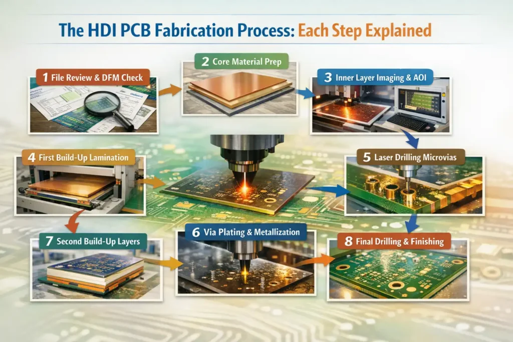
Step 1: File Review and DFM Check
Before any material is cut or drilled, the engineering team reviews your design files for manufacturability. This includes the Gerber or ODB++ file package, the drill file, the stack-up specification, any impedance control requirements, and via structure definitions.
The DFM check looks for issues that would reduce yield or cause rework. Common issues flagged at this stage include microvias with aspect ratios above 1 to 1, stacked via structures that exceed three levels vertically, trace widths below the process minimum, annular rings too narrow for reliable laser drilling registration, and stack-up specifications that are inconsistent with the material options available.
For HDI boards, a DFM review before production is not optional. Because each sequential build-up cycle is expensive and time-consuming to redo, catching a design issue before production starts saves significantly more time and cost than catching it after the first lamination cycle fails inspection. FastTurn PCB performs DFM review on every HDI order at no additional charge, with feedback typically returned within hours.
Step 2: Core Material Preparation
The starting point for every HDI board is a rigid core, which forms the center of the final stack. The core is a standard double-sided copper-clad laminate made from FR4 or a specialty material. High-speed designs may use low-loss cores with better dielectric properties. Automotive applications typically specify high Tg FR4 or halogen-free laminates for improved thermal performance and environmental compliance.
The core is cut to panel size, cleaned, and inspected before any imaging begins. Panel dimensions are chosen to maximize the number of boards per panel while leaving room for tooling holes, registration targets, test coupons, and edge rails for handling through the production line.
Step 3: Inner Layer Imaging
Inner copper layers are imaged using Laser Direct Imaging. An LDI system projects the circuit pattern directly onto the photoresist-coated copper surface using a UV laser controlled by your Gerber data, without requiring a physical photomask. This gives LDI significant advantages over older contact-exposure systems: the laser-defined pattern is sharper, registration between layers is tighter, and line widths below 3 mil are achievable with consistent results across the panel.
After LDI exposure, the photoresist is developed, the exposed copper is chemically etched away, and the remaining resist is stripped. What remains is the copper circuit pattern for that layer. Each inner layer is inspected by automated optical inspection before lamination so that defective layers can be identified and removed before they are buried inside the board.
👉 You might also like: The SaaS Trap: How Startups Can Optimize Their 2026 Software Budgets with Perpetual Licensing
Step 4: Inner Layer Inspection by AOI
Every inner layer goes through automated optical inspection immediately after etching. AOI equipment scans the copper pattern at high resolution and compares it to the reference data from your Gerber files. It detects open circuits where copper is missing, short circuits where copper bridges across gaps, and dimensional deviations in trace widths or spacing.
Catching inner-layer defects at this stage is critical. Once layers are laminated together, the inner copper is inaccessible. A short or open buried in the laminate cannot be reworked. Every defective inner layer found at AOI is either repaired if possible or removed from the panel and replaced before lamination proceeds.
Step 5: First Sequential Build-up Lamination
Once the core inner layers pass inspection, the first sequential build-up lamination begins. A thin dielectric film is applied to each side of the core. In HDI production, two common materials are used for build-up dielectric: Resin Coated Copper, which is a thin copper foil bonded to a layer of resin, or laser-drillable prepreg, which is a thinner and more uniform fiber-reinforced material.
The build-up layers are pressed onto the core under controlled temperature, pressure, and vacuum to bond the dielectric to the core copper and eliminate voids. The dielectric thickness at this stage is tightly controlled because it directly determines the laser drilling depth, the coupling between adjacent copper layers, and the impedance of traces routed on the build-up layer.
For a standard 1+N+1 HDI board, one build-up layer is applied to each side of the core. For 2+N+2 and higher structures, the first build-up cycle produces one layer on each side, and the process repeats after laser drilling, plating, and imaging to add the second build-up layer.
Step 6: Laser Drilling of Microvias
After the first build-up lamination, microvias are formed by laser drilling. A UV or CO2 laser ablates through the thin dielectric layer, removing material between the outer copper surface of the build-up layer and the copper pad on the layer below. The result is a precise conical opening, typically 100 micrometers in diameter at the top surface.
The laser is controlled by your drill file data. Each microvia position is drilled by firing the laser at the exact coordinates of the corresponding pad on the underlying layer. Because microvias connect only adjacent layers, the laser only needs to remove one dielectric layer at a time. This is different from mechanical drilling, where a drill bit passes all the way through the board stack.
Laser drilling is significantly more precise than mechanical drilling for small diameters. Mechanical drill bits are not practical below about 0.15 mm finished hole diameter. Laser drilling routinely achieves 100-micrometer microvias with tight positional accuracy, enabling the via-in-pad structures and fine pitch BGA routing that define HDI capability.
After laser drilling, a desmear process chemically cleans the via walls and removes resin residue that would interfere with copper plating adhesion. The cleaned vias are then ready for metallization.
👉 You might also like: Robotics and Automation: Changing the Workforce and Everyday Life
Step 7: Via Metallization and Copper Plating
Laser-drilled microvias have walls of dielectric material that do not conduct electricity. To make them electrically conductive, the via walls are first seeded with a very thin layer of copper by electroless deposition. In this process, the panel is immersed in a chemical bath that deposits copper uniformly on all exposed surfaces, including the via walls, without requiring an electrical current.
After the electroless seed layer is established, the panel goes through electrolytic copper plating. An electrical current drives copper ions from the plating solution onto the seeded surfaces, building up the copper to the required wall thickness. Standard microvia plating targets a minimum wall thickness that meets IPC-6016 requirements for the reliability class of your application.
For via-in-pad structures, the microvias are completely filled with copper or epoxy rather than just wall-plated. Copper fill uses a specialized plating process that overfills the via, then the surface is planarized by micro-etching or mechanical polishing to bring the filled via flush with the surrounding copper. FastTurn PCB achieves surface planarity within 10 micrometers on via-in-pad structures, which is the tolerance needed for reliable BGA assembly on 0.4 mm pitch pads.
Step 8: Outer Layer Imaging and Etching of Build-up Layer
After via metallization, the copper surface of the build-up layer is imaged by LDI and etched to form the circuit pattern for that layer. The process is the same as inner layer imaging: photoresist is applied, LDI exposes the circuit pattern, resist is developed, unwanted copper is etched, and resist is stripped.
Trace widths on HDI build-up layers are typically 2.5 to 3 mil, significantly finer than the 5 mil or wider traces commonly used on standard multilayer boards. LDI imaging is essential at these trace widths because contact exposure systems do not have the resolution or registration accuracy to reliably produce 2.5 mil traces across a full production panel.
After imaging and etching, the build-up layer surface is inspected by AOI before the next lamination cycle begins.
Step 9: Sequential Repetition for Additional Build-up Layers
For HDI boards with two or more build-up layers on each side, the lamination, laser drilling, metallization, imaging, and inspection cycle repeats for each additional layer. The second build-up layer is laminated on top of the first, laser-drilled to form microvias connecting to the first build-up layer below, plated, imaged, and inspected before the third cycle begins.
Registration between cycles is one of the most critical process controls in multi-cycle HDI fabrication. Each microvia pad on the new build-up layer must align precisely with the copper feature on the layer directly below. FastTurn PCB uses optical registration systems with fiducial targets on each layer, maintaining layer-to-layer registration within 50 micrometers across the full panel. At this tolerance, stacked microvias line up reliably, and the annular ring around each via pad remains intact on every layer.
For any-layer HDI, where every layer in the board is a build-up layer, this cycle continues until all layers are complete. Any-layer structures require the highest manufacturing capability because registration errors accumulate with each additional cycle and must be controlled at every stage.
👉 You might also like: 5 Best AI Tools for Automating Business Tasks in 2026
Step 10: Final Core Lamination
After all build-up cycles on both sides of the core are complete, the board goes through a final outer lamination step. For boards where the core itself carries buried vias between inner layers, those vias were formed and plated in earlier processing steps before the build-up layers were added. At this stage, the completed build-up structure on both sides of the core is ready for the final outer layer processing.
Step 11: Final Outer Layer Drilling and Plating
Plated through-holes that pass through the entire board, connecting the top outer layer to the bottom outer layer or to inner layers, are drilled mechanically at this stage. These are not microvias. They are standard through-holes for component leads, tooling holes, and board-level interconnects that require connection across the full board thickness.
Mechanical drilling at this stage uses tungsten carbide drill bits at high rotation speeds, typically 100,000 to 200,000 RPM, with drill diameters from 0.15 mm upward. The finished hole diameter after plating at FastTurn PCB starts at 0.15 mm. After drilling, through-holes go through desmear and the same electroless and electrolytic copper plating process used for microvias, building the copper barrel inside each hole to the required wall thickness.
Step 12: Final Outer Layer Imaging and Etching
The final outer copper layers are imaged by LDI and etched to form the top and bottom circuit patterns. This is the same process as inner layer and build-up layer imaging, applied to the outer layers that will carry the component pads, surface mount lands, test points, and any exposed copper features visible on the finished board.
Step 13: Soldermask Application and Imaging
Liquid photoimageable soldermask is applied to both sides of the board, covering the copper traces and leaving only the component pads and through-hole barrels exposed. The soldermask is imaged by UV exposure through a film or by LDI, then developed to open the pad openings precisely.
Soldermask serves two functions. It protects copper traces from oxidation and contamination during the board’s service life. It also prevents solder bridging between adjacent pads during assembly by confining solder flow to the exposed pad openings. Soldermask opening size and registration to the underlying copper pads are critical for reliable assembly, particularly on fine-pitch pads.
👉 You might also like: 5 Best Platforms for Building SaaS Applications in 2026
Step 14: Surface Finish
The exposed copper pads receive a surface finish to protect them from oxidation before assembly and to provide a solderable surface. The most common finish at FastTurn PCB is Electroless Nickel Immersion Gold, which deposits a thin layer of nickel followed by a thin layer of gold on each exposed copper pad. ENIG provides a flat, solderable, and wire-bondable surface that is compatible with most assembly processes and shelf-stable for extended storage.
Other available finishes include HASL lead-free, immersion silver, immersion tin, and selective hard gold for edge connectors and contact wear areas. HASL is the fastest and lowest-cost option. Immersion silver and immersion tin provide flat surfaces for fine-pitch assembly. Hard gold is specified for high-wear contact areas such as edge connectors and gold fingers.
Step 15: Electrical Testing
Every finished board undergoes 100 percent electrical testing. Flying probe testers contact each net on the board and verify continuity and isolation. The test compares the measured connectivity of the fabricated board to the netlist derived from your design files. Any net that shows an open circuit or a short to another net fails the test.
For boards with controlled impedance requirements, time-domain reflectometry testing is performed on test coupons included in the panel. TDR measures the actual impedance of traces and compares it to the specified target. FastTurn PCB holds controlled impedance to plus or minus 5 ohms or plus or minus 10 percent, with TDR test reports provided with the shipment.
Step 16: Final Inspection, Profiling, and Shipment
After electrical testing, boards go through a final visual inspection and automated optical inspection of the outer layers. Soldermask coverage, surface finish quality, silkscreen legibility, and board dimensions are checked against your acceptance criteria.
Boards are then profiled to final dimensions by CNC routing or scoring, depending on your panelization method. Individual boards are separated from the panel, inspected for edge quality, and packed in ESD-safe packaging with moisture barrier bags for moisture-sensitive designs. Full documentation, including test reports, certificates of conformance, and traceability records, ships with every order.
Key Specifications That Define HDI Fabrication Capability
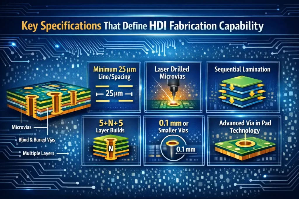
When evaluating whether a supplier can produce your design, these are the numbers to verify:
- Minimum microvia diameter: 100 micrometers at FastTurn PCB. Microvias below this diameter require specialized laser equipment and tighter process controls.
- Minimum trace and space: 2.5 mil at FastTurn PCB for production builds. This is achievable with LDI imaging and is at the practical limit of standard wet etch processing.
- Minimum plated through-hole: 0.15 mm finished diameter at FastTurn PCB. Below this diameter, mechanical drilling is not reliable, and laser drilling of through-holes would be required.
- Layer-to-layer registration: Within 50 micrometers at FastTurn PCB. This tolerance determines whether stacked microvias align reliably across multiple build-up cycles.
- Via fill planarity: Within 10 micrometers at FastTurn PCB for filled via-in-pad structures. This surface flatness is required for reliable BGA assembly on fine pitch pads.
- Controlled impedance tolerance: Plus or minus 5 ohms or plus or minus 10 percent at FastTurn PCB, verified by TDR testing on panel coupons.
- Maximum build-up layers: 18 HDI build-up layers at FastTurn PCB, with a total layer count up to 32. Ask any supplier to provide build records for the specific layer count and structure you need.
Material Options for HDI Fabrication
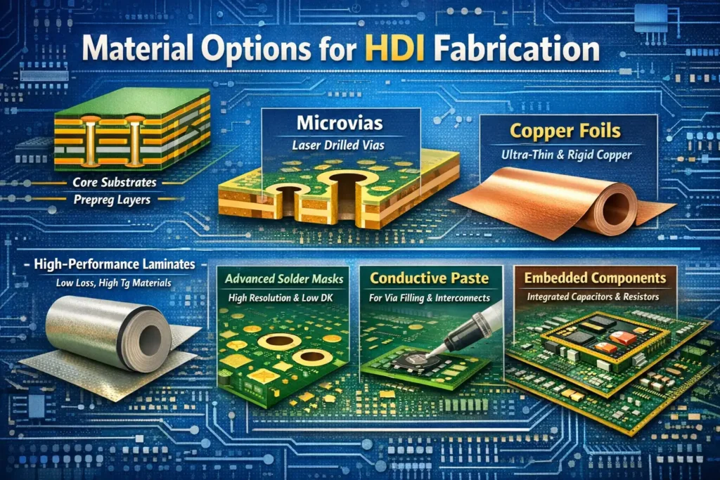
Material selection for HDI boards depends on your electrical performance requirements, operating environment, and regulatory compliance needs.
Standard high Tg FR4
Used for most HDI applications. High Tg materials withstand the multiple reflow cycles of assembly and the thermal stress of sequential build-up lamination better than standard Tg FR4. FastTurn PCB uses high Tg FR4 as the default core and build-up material for HDI builds.
Halogen-free laminates
Required for automotive, industrial, and many European market applications where environmental compliance standards restrict halogenated flame retardants. Halogen-free materials meet IEC 61249-2-21 requirements and provide similar electrical properties to standard FR4.
Mixed dielectric stack-ups
For high-speed designs operating above 10 Gbps, the signal loss in standard FR4 becomes a limiting factor. Mixed stack-ups combine standard FR4 for layers where signal performance is not critical with low-loss cores on the layers carrying high-speed differential pairs. FastTurn PCB supports mixed dielectric builds combining FR4 with low-loss materials for designs where FR4 alone cannot meet the insertion loss budget.
Polyimide
Used for rigid boards that need to operate at temperatures well above the capabilities of FR4, or for boards requiring exceptional dimensional stability. Polyimide builds take longer than FR4 and cost more, but are the correct choice for demanding thermal environments.
Common HDI Fabrication Questions
How long does HDI PCB fabrication take?
FastTurn PCB offers 24 to 48 hour prototype turnaround for standard HDI structures such as 1+N+1 and 2+N+2 when design files are complete, and materials are available. More complex structures with higher build-up layer counts take 5 to 10 business days. Production quantities have lead times confirmed at order placement based on volume and complexity.
What files do I need to submit for an HDI order?
You need Gerber files in RS-274X or ODB++ format for all layers, including build-up layers and core inner layers, a drill file specifying microvia and through-hole positions and diameters separately, a stack-up document describing layer sequence, dielectric materials, copper weights, and total finished thickness, and any controlled impedance specifications with target values and reference layers. Assembly orders also require a BOM and pick-and-place centroid file.
Does FastTurn PCB require a minimum order quantity for HDI?
No. FastTurn PCB builds HDI boards from single prototype quantities through medium volume production runs. Prototype pricing applies to small quantities and scales with complexity rather than volume. There is no minimum order quantity requirement.
What certifications apply to HDI boards from FastTurn PCB?
ISO 9001 covers the quality management system across all production. ISO 13485 covers medical device manufacturing. UL certification, RoHS compliance, and REACH compliance apply to materials and processes. Boards are inspected and tested to IPC-A-600 and IPC-6012 standards, and assemblies follow IPC-A-610 Class 2 or Class 3, depending on your specification.
Conclusion
HDI PCB fabrication involves more process steps, tighter tolerances, and more specialized equipment than standard multilayer fabrication. Each stage from DFM review through final electrical test plays a specific role in ensuring the finished board meets its design intent and works reliably in the application.
For engineers preparing their first HDI design, the most important steps you control are submitting complete design files with a clearly defined stack-up, specifying your via structures explicitly in the drill file, confirming that your trace widths and via dimensions are within the process window of your chosen supplier, and including impedance test coupons on your panel if your design has controlled impedance requirements.
FastTurn PCB has built HDI boards across medical, automotive, telecom, and consumer electronics applications since 2015. Every HDI order receives a free DFM review before production begins, with feedback typically returned the same day.
To get a quote and DFM review for your next board, visit HDI PCB fabrication services at FastTurn PCB and upload your files for a same-day engineering review.
✨ More clarity. More insights. Less noise. Follow Tech Statar.


")


